
The deep dive into HBM3 manufacturing: The evolution of memory technology
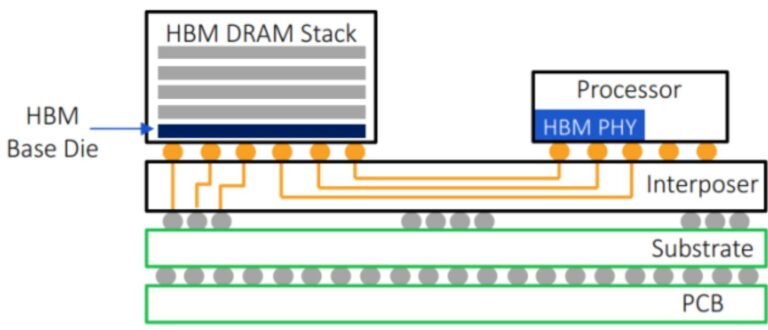
HBM3 (High Bandwidth Memory 3) is a high-performance type of DRAM used in advanced computing applications like AI, high-performance computing (HPC), and graphics processing. The architecture of HBM3 involves multiple DRAM dies stacked vertically, connected through-silicon vias (TSVs) for high data transfer rates. These memory stacks are mounted on a silicon interposer, which serves as a bridge between the HBM3 memory and the processor, such as a GPU, CPU, or FPGA. The manufacturing process of HBM3 is highly complex, involving the fabrication of DRAM dies using advanced semiconductor processes, often at 7nm or smaller nodes. These dies are then stacked vertically and connected using TSVs, allowing for a smaller footprint and reduced latency.
In HBM3 manufacturing, wafer-level packaging plays a crucial role, where the DRAM stacks are assembled and tested at the wafer level before being diced into individual units. The integration of multiple DRAM dies in a 3D stack requires advanced bonding techniques, like hybrid bonding or microbump technology, to ensure high electrical and thermal performance. Thermal management is another critical aspect, as the high power density of HBM3 necessitates effective cooling methods, such as micro-cooling and the use of thermal interface materials (TIMs).
Testing and validation are rigorous in HBM3 manufacturing, with extensive testing at various stages to ensure reliability, performance, and yield. This includes electrical and thermal testing, as well as performance validation.