Fins to Fails: Layout/PnR Lessons at Advanced Nodes
Designing at lower nodes isn’t just “same thing but smaller.” Here’s a breakdown of the real-world layout challenges:
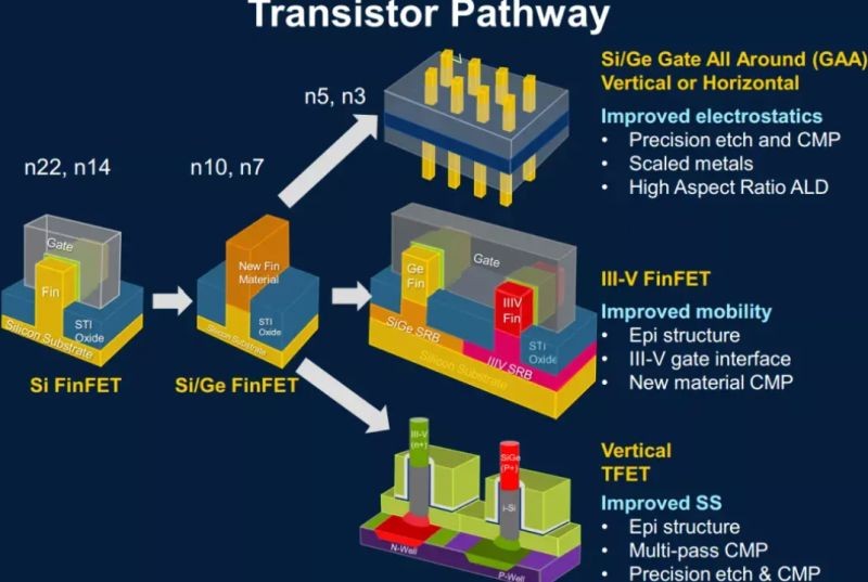
FinFET_Geometry_Constraints:
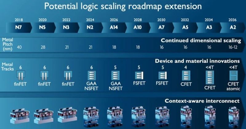
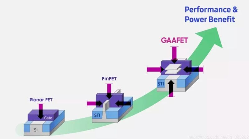
With 3nm/5nm being FinFET-based, transistor placement isn’t just about symmetry or matching anymore—it’s about fin quantization. You can only place devices on predefined fin grids, and your fingers are counted.
EUV lithography tightens rules further. Even small misalignments can cause fatal errors, so grid snapping and layer coloring becomes critical.
Restricted_Design_Rules:
These nodes come with hyper-dense RDRs:
Track-based routing (no free-form routes like older nodes)
Color-aware metal rules (double-patterning and EUV constraints)
Cut layers and via enclosures are extremely tight and complex
You spend more time solving local DRCs around vias and abutments than drawing the actual shapes!
Increased_Parasitic_Sensitivity:
At 3nm, even a few extra fF or mΩ can seriously degrade performance. This makes shielding, via optimization, and device placement symmetry more critical than ever.
Floorplan has to be parasitic-aware, especially in high-speed analog (e.g., PLLs, SERDES).
EM_IR_Compliance is Brutal:
Smaller widths and tighter pitches → higher resistance and lower current handling. Need to over-provision metal and vias to stay within EM specs, even if it hurts area. Strap planning, power rail staggering, and dedicated guard rings are essential
Device_Variability & Matching:
Matching across orientation and local stress effects (caused by dummy poly, fin density imbalance) becomes unpredictable.
You often need custom dummy fill strategies, not just default PDK rules, especially in analog blocks like Bandgaps, VCOs, or Bias Generators.
LVS_DRC Runtime & Debug:
DRC decks for 3nm are enormous. Each DRC/LVS run takes longer, and violations are trickier to debug.
Even simple cell-level designs can throw odd coloring, enclosure, or via redundancy issues that didn’t exist in older nodes.
Takeaway:
🔹 Device architecture has changed – FinFETs bring in quantization issues, mismatch behavior shifts, and layout-dependent effects that are far more critical than just rule compliance.
🔹 Parasitics dominate – At these scales, parasitics can wreck performance if not planned carefully, especially in analog blocks like VCOs, CTLEs, and bandgaps.
🔹 Shielding and spacing – Noise coupling becomes brutal. It’s no longer just about shielding; it’s strategic placement of routing, devices, and even dummy structures.
🔹 DFM and variability – Lower-node fabs are sensitive to systematic variation, so your layout style can directly impact yield.
🔹 Complex checks – Things like DPT (Double Patterning), EM/IR, via redundancy, and reliability checks can be just as important as LVS/DRC.