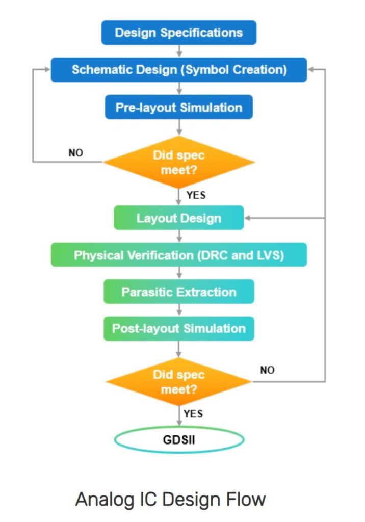
Post-Layout Simulation Validates Circuit Design
Post-layout simulations are a crucial step in the design flow for integrated circuits (ICs), especially in analog and mixed-signal designs:
Overview of Post-Layout Simulation:
Objective: To verify the behavior and performance of the circuit after the layout process, including parasitic capacitance, resistance, and inductance that are introduced during physical design.
Key Factors: Parasitic elements, foundry process variations, and design rules are considered to ensure the design functions as intended in the final physical form.
Types of Post-Layout Simulations:
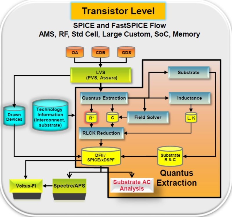
RC Extraction: This step involves extracting parasitic resistances and capacitances from the layout. These parasitics are then incorporated into the circuit model for simulation.
Signal Integrity Simulations: Ensure that signal quality is maintained after the layout. This includes simulations of crosstalk, reflection, and noise that could affect the performance.
Timing Analysis: In digital designs, it’s essential to simulate the effects of layout on the timing of signal transitions, such as setup and hold times.
Voltage and Current Analysis: Simulate the supply voltage and current behavior, especially under different load conditions, to identify potential issues like voltage drops or current starvation.
Thermal Simulations: Some tools also simulate heat dissipation and thermal effects, which can affect performance and reliability.
Power Integrity Analysis: This is crucial in high-speed and high-frequency designs to ensure that power delivery to various components in the layout remains stable and efficient.
Post_Layout Simulation Flow:
Layout Extraction: After the layout is completed, extraction tools generate an accurate netlist that includes the parasitic elements (resistance, capacitance, and inductance) added by the physical layout.
Simulate with Parasitics: This new netlist with parasitics is used for post-layout simulation using tools like SPICE or other specialized simulators (e.g., Cadence Spectre, Mentor Graphics, etc.).
Verification: The circuit’s functionality is checked for any discrepancies between pre-layout and post-layout performance, including timing violations, voltage irregularities, and other electrical failures.
Iterate: Based on the simulation results, the design may need to be modified (e.g., adjusting transistor sizes, changing routing, or optimizing power delivery) and re-simulated until the desired performance is achieved.
Importance of Post-Layout Simulations:
Accurate Design Verification: Ensures that the final design will meet performance specifications after the manufacturing process.
Avoids Costly Mistakes: Detecting issues in the post-layout phase can prevent costly rework or redesigns in later stages.
Optimizes Design for Manufacturing: Helps ensure that the design will function correctly across variations in manufacturing processes.