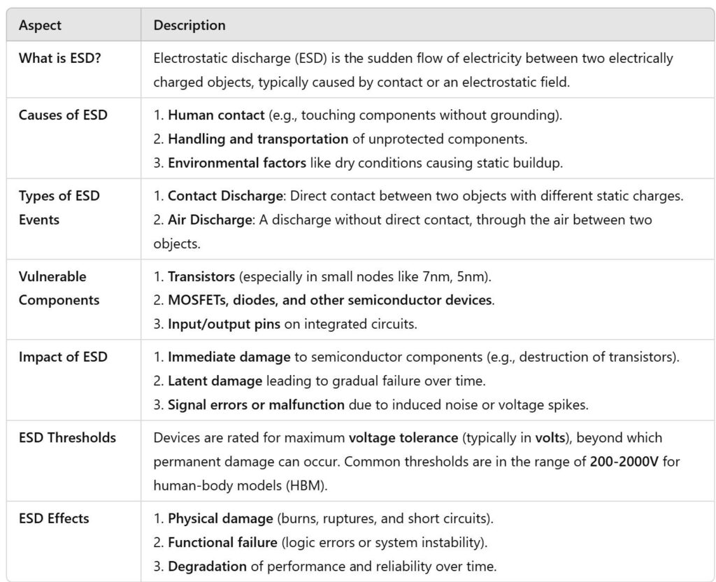
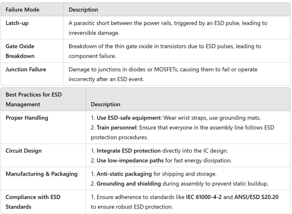
ESD is a sudden and uncontrolled flow of electricity between two electrically charged objects, often caused by direct contact or an electrostatic field. In circuit design, ESD protection is crucial because it can cause:
1. Immediate damage:
ESD can destroy sensitive components, like transistors, by exceeding their voltage tolerance, potentially causing permanent failure.
2. Degradation over time:
Even if immediate failure doesn’t occur, repeated exposure to ESD can cause latent damage that degrades the performance and reliability of components over time.
3. Interference:
ESD events can induce noise in circuits, leading to logical errors, instability, or malfunction in highprecision applications.
4. Failure in highstakes industries:
In sectors like automotive, aerospace, medical, and consumer electronics, where reliability is critical, ESDrelated failures can lead to costly recalls, safety risks, and longterm system outages.
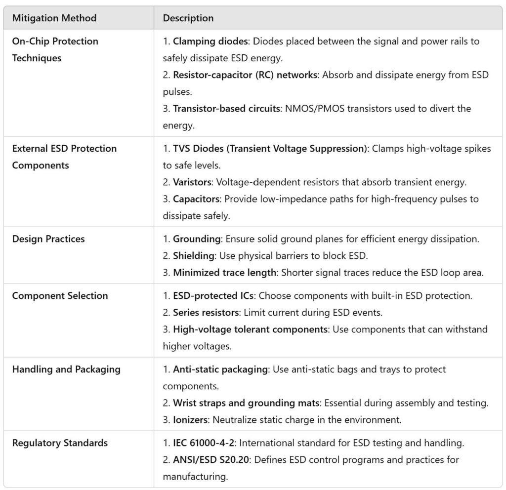
Methods to Mitigate ESD in Circuit Design
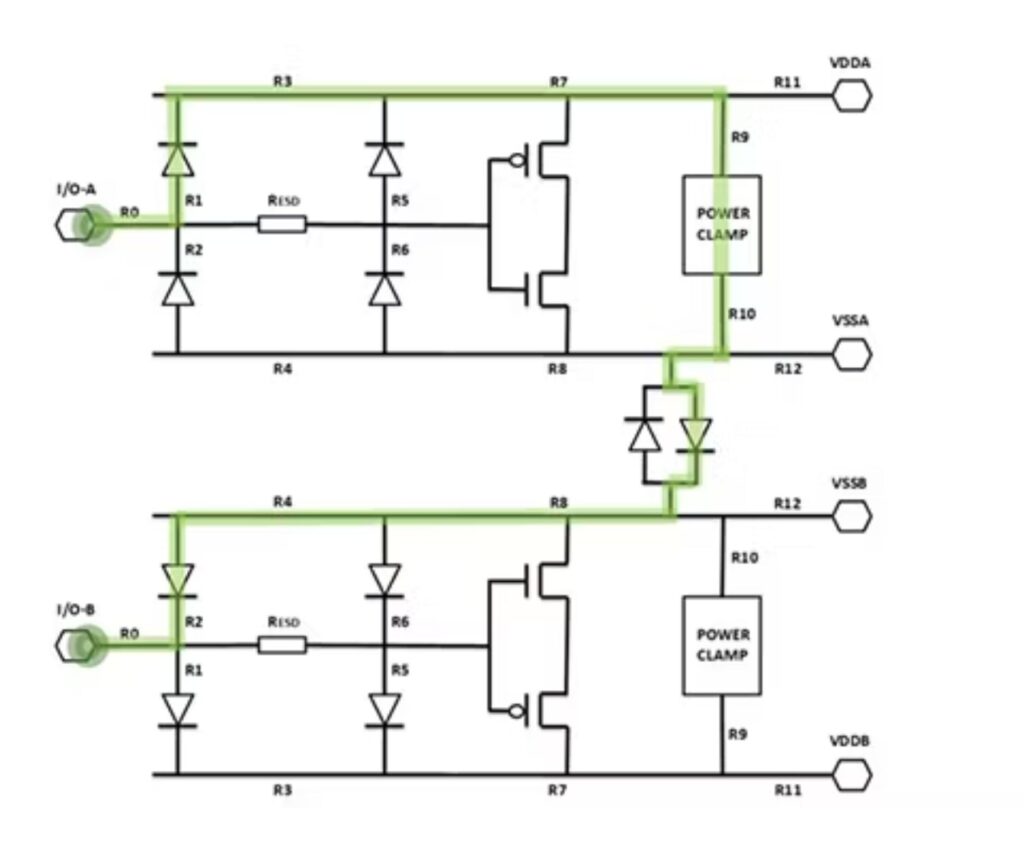
OnChip_Protection
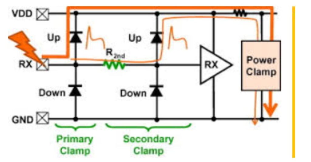
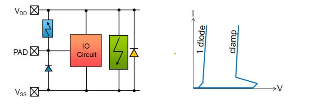
Clamping Diodes: These diodes are placed between the signal lines and the power rails to shunt the ESD pulse away from the sensitive parts of the circuit. When an ESD event occurs, the diodes conduct and clamp the voltage to a safe level, preventing damage.
Transistorbased Protection: NMOS or PMOS transistors can be used to create voltage clamping circuits. These transistors turn on during an ESD event, diverting the current to a safe path.
Resistors and Capacitors: RLC devices can be added to provide current limiting and energy dissipation to absorb some of the ESD energy.
External_ESD_Protection_Components
In addition to onchip protection, external protection components are often added to circuits to protect against ESD events,
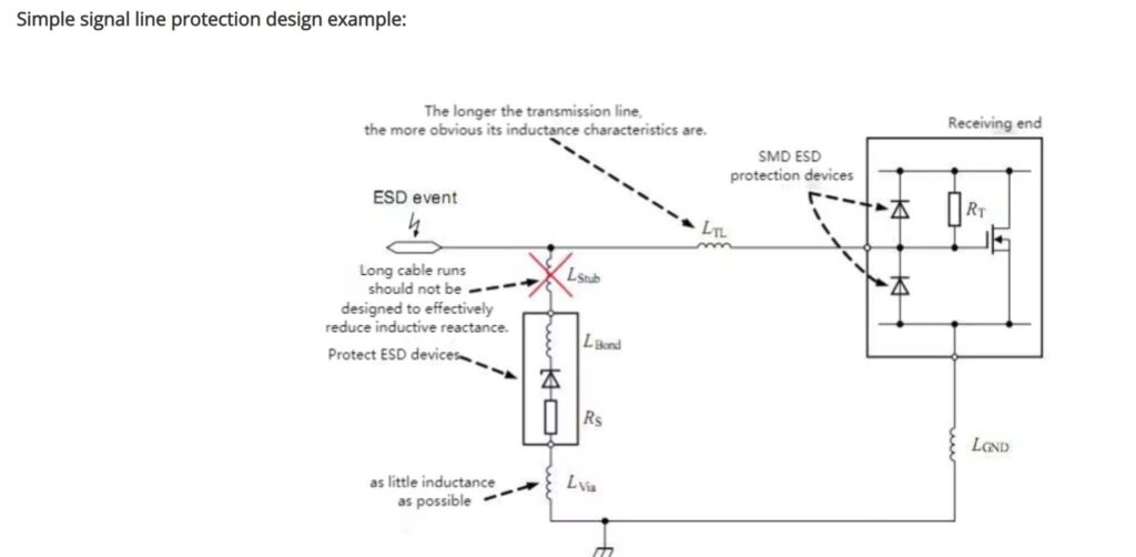
TVS Diodes: TVS diodes are widely used for external ESD protection. They are designed to clamp highvoltage transients to safe levels, protecting sensitive circuit components. These diodes can be placed at the input/output pins of a device or at critical nodes.
Capacitors: A capacitor can be placed in parallel with the sensitive components to provide a lowimpedance path to ground for the ESD energy, helping to absorb the pulse.
Design_Robustness
PCB Grounding and Shielding: Proper grounding and shielding can help divert ESD energy away from sensitive parts of the circuit.
Minimize Loop Areas: Minimize the area of the loop formed by the ESD path between the input pins and ground. Larger loops can act as antennas, amplifying the ESD signal.