
Additional aspects on HBM3 manufacturing
Fabricating FinFETs involves several intricate steps, especially when aiming to integrate High Bandwidth Memory I/O (HBMIO). FinFET technology, being a type of 3D transistor, requires precise processing techniques to achieve the desired performance and density. Here’s an overview of the typical steps involved in FinFET fabrication, particularly for applications involving HBMIO:
Wafer Preparation and Oxidation:
The process starts with the preparation of a high-quality silicon wafer, which serves as the substrate. A thin layer of silicon dioxide is grown on the wafer’s surface through thermal oxidation. This layer functions as an insulating barrier for the gate in the FinFET structure.
Photolithography and Etching:
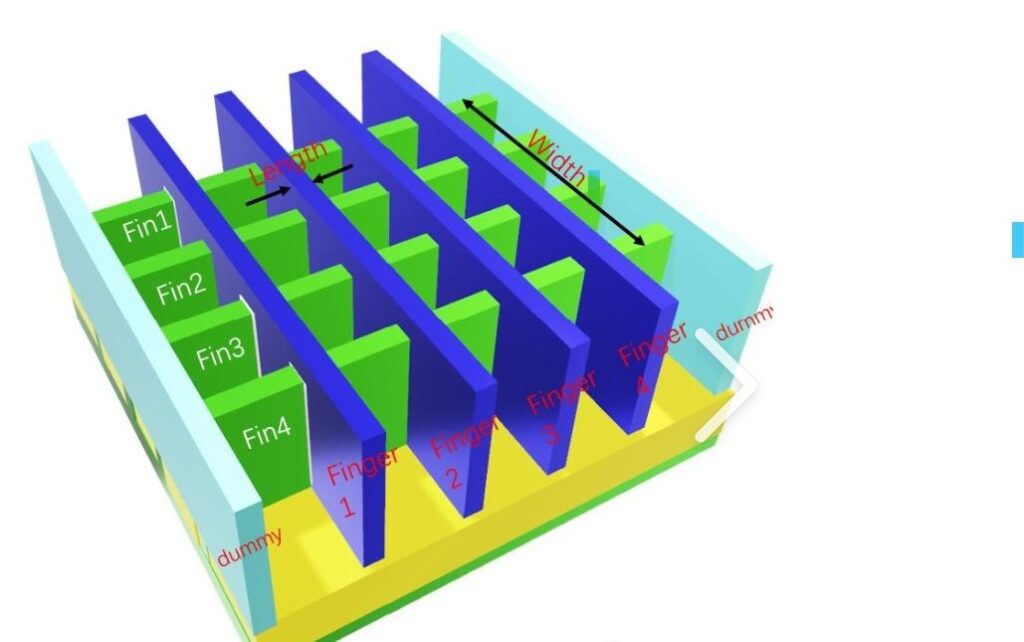
Next, the wafer is coated with a photoresist material, which is then exposed to ultraviolet light through a photolithography mask. This process patterns the photoresist layer to define regions for subsequent etching. After exposure, the wafer undergoes etching to remove the exposed silicon dioxide and silicon, thereby forming the vertical fins that are characteristic of FinFET transistors. The fins are essential for creating the three-dimensional structure that improves transistor performance.
Gate Formation:
With the fins in place, the next step involves the formation of the gate structure. A high-k dielectric material is deposited over the fins to create the gate dielectric, enhancing the transistor’s electrical properties. Following this, a gate electrode material—typically metal or polysilicon—is deposited and patterned to form the transistor gates. This step is crucial for defining the electrical characteristics of the FinFETs.
Source/Drain Formation and Contact Creation:
The source and drain regions are created through ion implantation, where dopants are introduced into the areas around the fins. This is followed by an annealing process to activate the dopants and repair any damage caused during implantation. After this, contact holes are etched through the insulating layers to expose the source and drain regions. Metal is then deposited and patterned to form electrical contacts to these regions, enabling connectivity for the transistor.
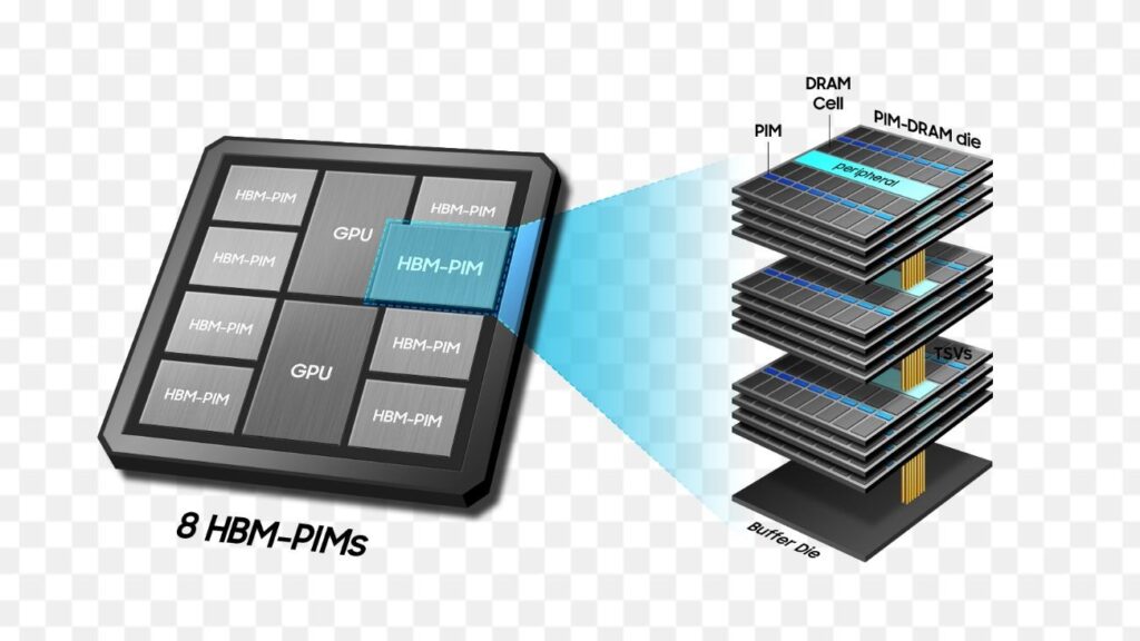
HBMIO Integration, Testing, and Packaging:
Integrating HBMIO requires additional layers and precise alignment to bond memory stacks with the logic wafer. Through-Silicon Vias (TSVs) are created to enable vertical electrical connections between memory and logic layers. Once integration is complete, the wafer undergoes initial testing to identify any defects. The wafer is then diced into individual chips, which are packaged to protect them and facilitate connections. Finally, each chip is subject to rigorous functional testing to ensure it meets performance standards and operates correctly.